The race to rebuild America’s semiconductor supply chain is gaining momentum, but critical gaps remain in the final stages of chip production. Nvidia and Intel are aggressively expanding domestic manufacturing, yet the most advanced packaging steps for AI processors—where chips are assembled, tested, and stacked—still rely on facilities outside the U.S.
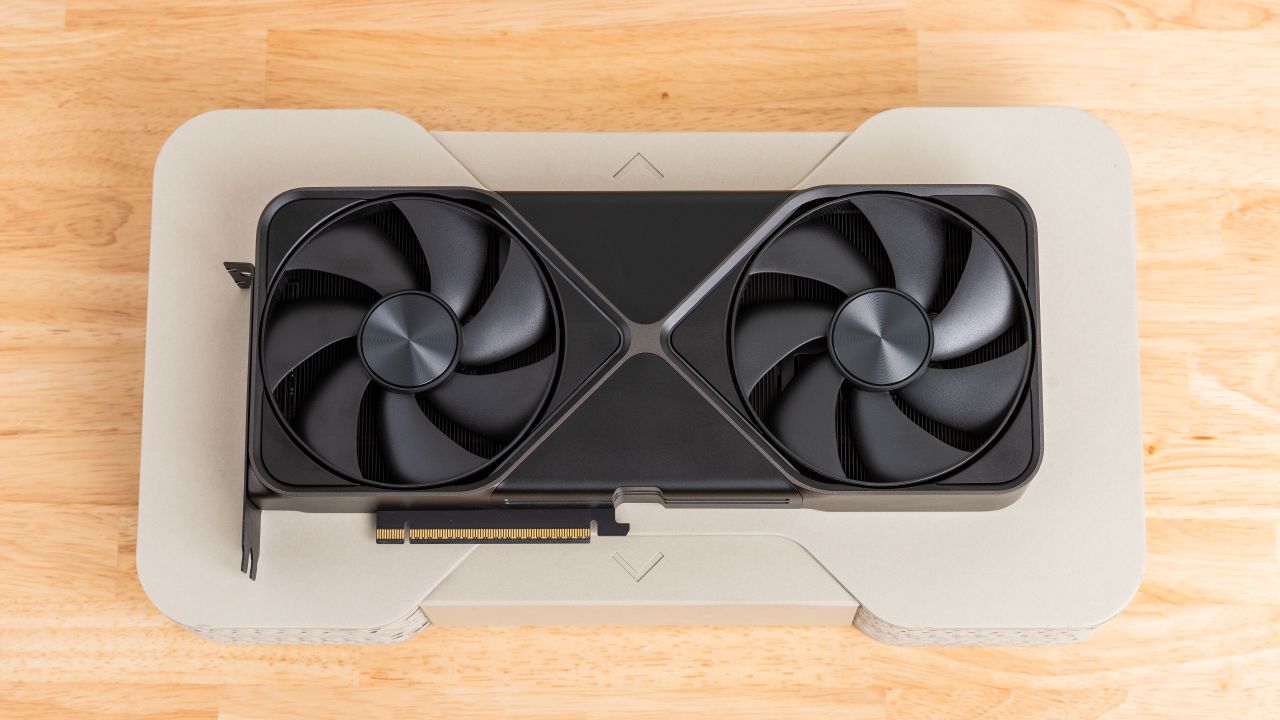
Nvidia recently highlighted its network of American manufacturing partners, claiming operations across 43 states and plans to produce up to $500 billion in AI infrastructure over four years. The company’s blog post emphasizes partnerships with TSMC, Foxconn, Wistron, Corning, Coherent, and Amkor, while Intel’s America 250 initiative touts end-to-end U.S. capabilities in design, manufacturing, and research. Both narratives celebrate progress, but they sidestep a persistent reality: the most advanced AI chips, including Nvidia’s Blackwell GPUs, still require overseas packaging before deployment.
Wafer production advances, but packaging lags
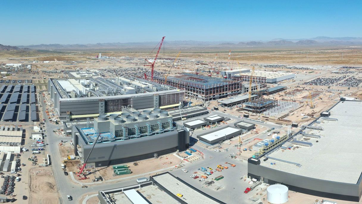
TSMC’s Phoenix facility has successfully transitioned to high-volume production of Blackwell silicon on its 4NP process—a custom 4nm-class node tailored for Nvidia. Meanwhile, Intel’s Fab 52 in Arizona has reached full operational capacity, producing Intel 18A wafers at a rate exceeding 10,000 starts per week. Panther Lake and Clearwater Forest processors have entered broad availability, with yields expected to stabilize by early 2027. These milestones mark a significant shift from the start of the decade, when advanced logic production in the U.S. was nearly nonexistent.
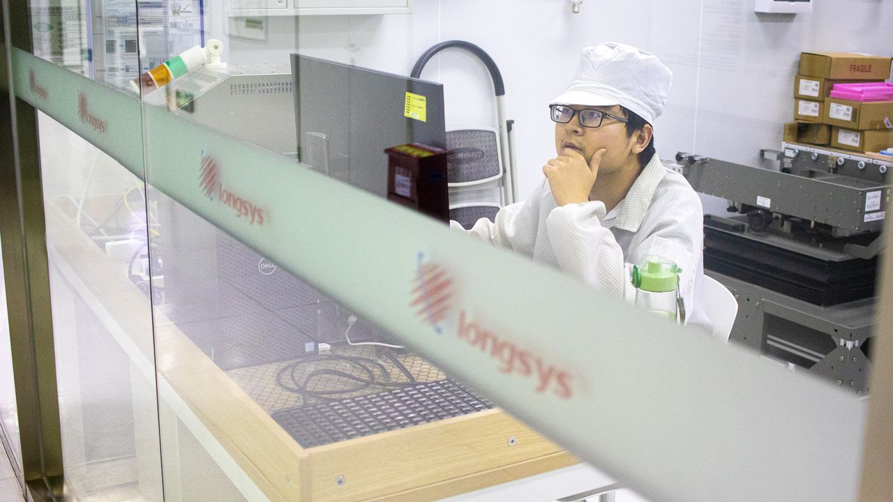
However, the journey from wafer to finished chip remains incomplete. A Blackwell data center GPU combines two compute dies with eight HBM3e stacks on a silicon interposer using TSMC’s CoWoS-L packaging. Every Blackwell die fabbed in Arizona must travel over 7,000 miles to Taiwan for final assembly, testing, and integration before returning for system deployment. This Pacific round-trip underscores a critical dependency on offshore packaging infrastructure.
HBM and advanced packaging still concentrated overseas
High Bandwidth Memory (HBM) stacks, essential for AI workloads, are currently produced exclusively in South Korea, Taiwan, and Japan. SK hynix and Samsung operate the primary HBM facilities, while Micron’s fabs in Taiwan and Japan supply additional capacity. Advanced organic build-up (ABF) substrates, which support interposer layers, are similarly concentrated in Japan and Taiwan. No U.S. facility currently manufactures or packages HBM, leaving a major gap in the domestic supply chain.
Intel stands as the sole major U.S. player with significant advanced packaging capabilities. Its Foveros operation in New Mexico handles 3D-stacked products and has reportedly attracted external interest, including Google’s booking of over 3 million TPUs for 2028 packaging. Notably, Intel does not appear in Nvidia’s list of manufacturing partners, highlighting a fragmented ecosystem.
New U.S. projects aim to bridge the gap—but not soon enough
Amkor’s $7 billion Peoria, Arizona campus, backed by $400 million in CHIPS Act funding, represents a major investment in domestic advanced packaging. Scheduled for completion in mid-2027 with production starting in early 2028, the facility aims to serve lead customers like Apple and Nvidia. TSMC has committed to a 10-year agreement with Amkor for packaging and test services, while TSMC’s own Arizona packaging plant is slated to begin operations before 2029.
SK hynix broke ground in April on a $3.87 billion advanced packaging facility in Indiana, though full-scale production is not expected before 2029. These projects signal long-term progress, but the timeline leaves a multi-year window where U.S.-fabricated AI chips will still depend on overseas packaging.
The road ahead: Can the U.S. close the packaging gap?
The current landscape reveals a paradox: the U.S. is making historic strides in wafer production, yet the final steps that transform silicon into shippable AI processors remain offshore. Nvidia projects that AI-driven demand will contribute $485 billion to U.S. GDP by 2026, supporting over 100,000 jobs. But without domestic advanced packaging capacity, this growth could face bottlenecks that delay deployment and increase costs.
Industry leaders acknowledge the challenge. Jensen Huang of Nvidia framed AI as "a once-in-a-generation opportunity to reinvigorate American manufacturing," yet the supply chain’s weakest link—packaging—remains unresolved. As new U.S. facilities come online, the next few years will determine whether the country can truly achieve self-sufficiency in AI chip production or remain tethered to global dependencies.
AI summary
NVIDIA ve Intel ABD’de yerli yarı iletken üretimini artırdığını iddia ediyor. Peki en gelişmiş yapay zeka çiplerinin paketlenmesi hâlâ neden yurt dışında yapılıyor? Kritik boşluklar neler?