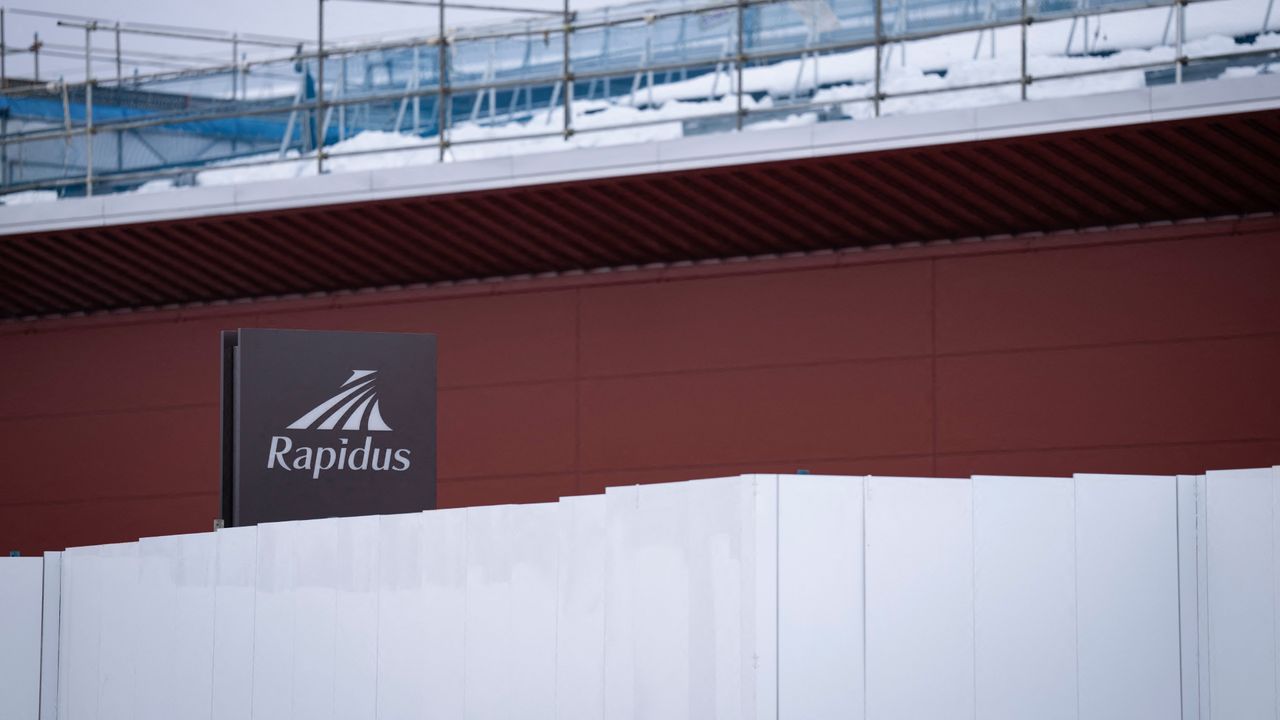
Japan’s semiconductor ambitions are on the line at Rapidus’s new facility in Chitose, Hokkaido. The company’s single fab, IIM-1, is the linchpin of the nation’s effort to reclaim a spot among the world’s leading-edge chipmakers. With a 2027 mass-production target for its 2nm process, Rapidus is operating on a tight schedule—and a high-stakes assumption that customers will follow through.
The clock is ticking on Japan’s 2nm gamble
IIM-1, or Innovative Integration for Manufacturing, broke ground in September 2023 and completed its cleanroom in 2024. The facility’s most critical milestone came in December 2024, when ASML delivered the first mass-production-grade EUV scanner installed in Japan. The tool began operations in April 2023, marking a first for the country’s chip industry. Since then, Rapidus has produced a 2nm gate-all-around prototype that met its expected electrical characteristics by July, according to company reports.
The timeline, however, remains fluid. Rapidus has set mass production for the second half of fiscal 2027, with full-scale output scaling to 2028. The company plans to ramp capacity from 6,000 wafer starts per month to 25,000 within a year, a fourfold increase aimed at reducing per-wafer costs. Yet, the absence of volume commitments from customers leaves the plan vulnerable—especially since IIM-1 is the only production site in Rapidus’s portfolio.
A 2nm process rooted in IBM’s legacy
Rapidus’s 2nm node leverages IBM’s gate-all-around nanosheet design, first announced in 2021. The company formed a strategic partnership with IBM in December 2022, allowing Rapidus engineers to collaborate at the Albany NanoTech Complex in New York. Between 2023 and 2024, over 150 Rapidus engineers trained at Albany, with roughly 80 later returning to Chitose to adapt the process for production.
The differentiator Rapidus emphasizes is its single-wafer front-end processing, branded as Rapid and Unified Manufacturing Service. Unlike batch processing used by rivals like TSMC and Samsung, Rapidus feeds per-wafer data into AI models to accelerate yield learning and reduce turnaround times. The company also claims its 2nm Process Design Kit reached early customers in Q1, though no yield figures have been published. Public updates so far confirm only that the prototype achieved expected electrical characteristics.
Beyond wafer fabrication, Rapidus is investing in chiplet and package design for 2nm-generation semiconductors. NEDO, Japan’s New Energy and Industrial Technology Development Organization, approved a fiscal 2026 budget to fund these efforts, including front-end and back-end technologies. The company has also hinted at panel-level glass-substrate packaging as part of its long-term roadmap, mirroring the integrated approach taken by Intel and Samsung.
Government backing and the stakes for Japan
Rapidus’s financial foundation is as ambitious as its technical goals. In February 2024, the company closed a ¥267.6 billion ($1.7 billion) funding round, with the Japanese government contributing ¥100 billion through the Information-technology Promotion Agency. The remaining ¥167.6 billion came from 32 private companies. This infusion made the government the largest shareholder, granting it veto power over key decisions, including share transfers and technology partnerships.
This round follows a larger commitment from November 2023, when Japan’s Ministry of Trade and Industry pledged approximately ¥1 trillion in support for fiscal 2026 and 2027, bringing total government backing to around ¥2.9 trillion. The scale of investment underscores the strategic importance of Rapidus to Japan’s economic and technological future.
Location, infrastructure, and the Hokkaido advantage
Chitose’s selection as the site for IIM-1 wasn’t arbitrary. The region offers critical resources for semiconductor manufacturing, including abundant water for wafer cleaning and a cool climate that reduces cooling loads. Hokkaido also boasts strong renewable energy potential, with wind, solar, and hydroelectric sources providing a sustainable power supply.
Local and prefectural authorities are rallying behind the project through the “Hokkaido Valley” initiative, which aims to create a semiconductor cluster spanning Tomakomai, Chitose, and Ishikari. The collaboration reflects a broader push to revitalize Japan’s chip industry by leveraging regional strengths and fostering an ecosystem of suppliers, research institutions, and skilled labor.
What’s next for Rapidus and Japan’s chip revival
Rapidus’s journey is a high-risk, high-reward proposition. The company’s success hinges on executing a flawless ramp to 2nm production while securing volume commitments from customers. With no fallback sites and a single facility at risk, the pressure is immense.
Yet, the stakes extend beyond Rapidus. Japan’s semiconductor revival is a matter of national pride and economic security. If the company meets its 2027 target, it could redefine the country’s role in global chip supply chains. If not, the consequences will ripple across industries and geopolitical strategies. For now, the world is watching Chitose—where the future of Japan’s chip industry is being written, one wafer at a time.
AI summary
Japonya’nın Rapidus şirketi, Hokkaido’daki Chitose tesisinde 2027’de devreye almayı planladığı 2nm prosesle yarı iletken üretiminde liderliğe oynuyor. Tek tesis stratejisi, riskler ve fırsatlar hakkında detaylar.